- 專利名稱(中文) / Polyimide表面金屬化技術
- 專利名稱(英文) / The Technology of Polyimide Surface Metallization
- 所屬單位(一級單位) / 工學院
- 所屬單位(二級單位) / 化學工程學系
- 發明人(中文) / 竇維平
- 發明人(英文) / Wei-Ping Dow
- 申請國家 /
- 專利類型 /
- 專利證書號 / I379919、I629375
- 技術成熟度 /
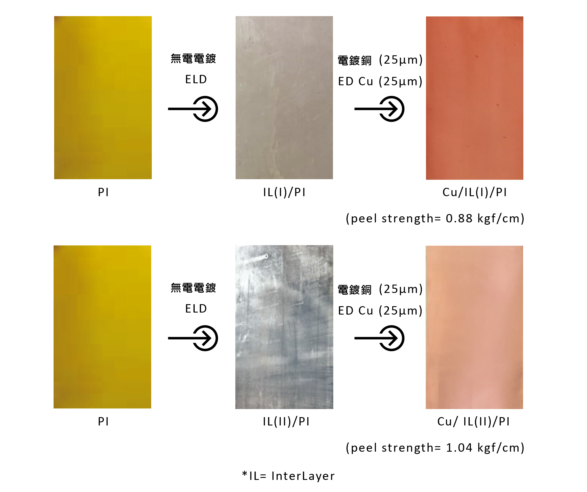
聚亞醯胺具有良好的耐熱性、電性、機械性質,且為一低介電長束之絕緣可撓性材料,故被廣泛應用於軟性電路板作為介電層。在軟性電路板製造過程中,聚亞醯胺須成為良好的導電材料。然而,銅線於軟性電路板上之寬度及空間大約為5微米,因此藉由SAP製程製造軟性電路板上之細間距線路。而此PI-SAP製程無須使用銅箔,可透過無電電鍍銅及電鍍銅直接進行導線之金屬化。也因為銅線在PI表面上是非常細小的,其黏著強度顯得相當關鍵。該技術使用全濕製程金屬化於PI薄膜,而上一層阻障層作為PI之阻障層後,進行電鍍銅箔。
Polyimide (PI) film is an insulator and has been commonly used as a dielectric layer of a flexible printed circuit board (FPCB) due to its high thermal stability, good mechanical strength, and excellent chemical resistance. For FPCB fabrication, PI is a dielectric layer which means its surface has to be metallized. However, the copper line width and space is about 5/5 micrometer on FPCB, so FPCB with fine pitch has to be manufactured by semi-additive process (SAP). PI-SAP will not use copper foil anymore. Instead, PI will directly be metallized by electroless deposition and then copper electroplating to form the conducting lines. Because the copper line on the PI surface is very thin and micro-scaled, the peeling strength is a very critical target in the metallization. In this study, we used an overall wet process to directly metallize the PI film. Plating a barrier layer was performed on a PI film as seed and barrier layer followed by copper electroplating.
聚亞醯胺、軟性電路板、無電電鍍銅、金屬化
Polyimide (PI)、Flexible Printed Circuit Board (FPCB)、Electroless Copper Deposition、Metallization